Circuit Simulation Part IV: Nonlinear circuits and implementation

In the last part  we presented the major part of the UI, but we still hadn’t talked about the implementation of solving. In this post we will talk about how to actually solve non-linear equations both in theory and in implementation.

Non-linear circuits

Since last time, I took a pass at cleaning up the code and I decided to implement a few more components (inductors and diodes).   Inductors were relatively easy since it is still linear, but the diode presented more problems. Let’s go through the theory of non-linear solves.

We started in Part I laying out how to devise an equation per KCL node. Each equation becomes a row in the matrix and then we just solve a linear system to get the final values. That’s all good and fine, but it only works for linear components like resistors, inductors, capacitors and simple source terms like voltages and currents. For things like diodes and transistors which have crap loads of annoying non-linear exponential crap in them, we are kinda screwed. So, we must turn to nonlinear solving techniques, in particular Newton-Raphson iteration which root solves non linear equations by solving linear approximations and iterating. Let’s do a brief overview to see what we’ll need. Let’s suppose the ith equation
\mathbf{F}_i(\mathbf{x}) = 0
But since \mathbf{F} this is nonlinear. So using the taylor approximation we can write an approximation to the function as
 \mathbf{F}_i(\mathbf{x}) \approx \mathbf{F}_i(\mathbf{x}^{n}) + \left. \frac{\partial \mathbf{F}}{\partial \mathbf{x}} \right|_{\mathbf{x}^n}\delta\mathbf{x}
where \delta\mathbf{x} = \mathbf{x}^{n+1} - \mathbf{x}^n and \partial\mathbf{F}/\partial\mathbf{x}|_{\mathbf{x}^n} is the Jacobian at the current iterate.
We still want the root to the approximation so we need to now solve
\mathbf{F}_i(\mathbf{x}^{n}) + \left. \frac{\partial \mathbf{F}}{\partial \mathbf{x}} \right|_{\mathbf{x}^n}\delta\mathbf{x} = 0
or specifically
 \left. \frac{\partial \mathbf{F}}{\partial \mathbf{x}} \right|_{\mathbf{x}^n}\delta\mathbf{x} = -\mathbf{F}_i(\mathbf{x}^{n})
Colloquially this is just a matrix equation \mathbf{A x}=\mathbf{b}. However, every Newton iteration we need to form a new A matrix. Thus given a current solution state \mathbf{x}_i we can go to a new one by following the steps:

  1. Solve  \left( \left. \frac{\partial \mathbf{F}}{\partial \mathbf{x}}\right|\mathbf{x}^n \right) \mathbf{\delta x}= -\mathbf{F}( \mathbf{x}^n )
  2. Update the solution to be \mathbf{x}^{n+1} = \mathbf{x}^n + \mathbf{\delta x}

On each time step we just repeat 1 and 2 as many times as needed for convergence given some norm. I just use check if \mathbf{\delta x} is small for now. So to implement this, we need a way to form the matrix, a way to compute derivatives and a way to solve matrices.

Implementation

Building a matrix

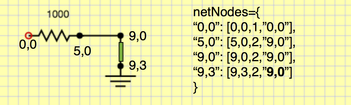
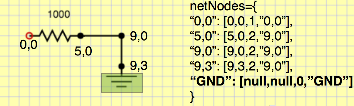
Conceptually, we need to form a matrix every time step and every Newton step. This requires two steps, identifying all the unknowns (which defines matrix dimensions), followed by determining the coefficients of the matrices. For various reasons (that probably are invalid and I will have to fix later) I thought it would be good to use separate objects for the solve and the UI. Thus, in the last segment we had a function that took “Symbol” objects and produced a final description like:

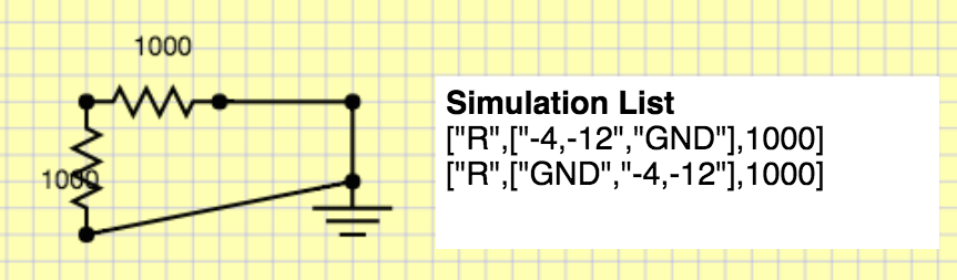
["R",["n1","n2"],1000]
["C",["n2","GND"],0.0001]
["V",["n1","GND"],"square,0.1,-1,1"]

We will go through the list and make “solver” objects now. It looks like this:

function createCircuitFromNetList(names,components){
    circuit=new Circuit();
    // Make a list of all the voltage nodes to graph
    namesToGraph=[]
    for(var n in names) namesToGraph.push(n);
    // Take visual components and turn them into simulation components
    for(var n in components){
        var node=components[n];
        switch(node[0]){
            case "R": circuit.addR(node[1][0],node[1][1],node[2]);break;
            case "C": circuit.addC(node[1][0],node[1][1],node[2]);break;
            case "V": circuit.addVoltage(node[1][0],node[1][1],node[2]);break;
            case "D": circuit.addD(node[1][0],node[1][1],node[2]);break;
            case "L": circuit.addI(node[1][0],node[1][1],node[2]);break;
        }
    }
    // solve and graph the circuit
    var foo=circuit.transient(3.0,.005,namesToGraph);
    graph(0,2,namesToGraph,foo);
}

Now essentially, we have connected up our UI part to our solver part. From here on out we are going to talk about the parts of the solver. It is possible to use those parts without a UI in a sense, so we basically have some compartmentalization!

Let’s look at what addR and addVoltage do because they are interesting:

Circuit.prototype.addVoltage=function(name1,name2,value){
    n1=this.allocNode(name1)
    n12=this.allocNode("sc"+this.num)
    n2=this.allocNode(name2)
    this.components.push(new Voltage(n1,n12,n2,value))
}
Circuit.prototype.addR=function(name1,name2,R){
    var n1=this.allocNode(name1)
    var n2=this.allocNode(name2);
    this.components.push(new Resistor(n1,n2,R))
}

The allocNode assigns that named node a number in the unknown vector. Once that is done, we make the component object using only the numbers. Each object knows how to contribute to the matrix and which values it contributes to. So in the example above we’d probably assign the matrix unknowns as [n1,n2,GND,sc3]. And remember these unknowns are going to actually be the delta in those values rather than the values themselves. Let’s look at how Resistor is implemented:

function Resistor(node1,node2,R){
    this.node1=node1
    this.node2=node2
    this.oneOverR=1.0/R
}
Resistor.prototype.matrix=function(dt, time, system, vPrev, xOld){
    system.addToMatrix(this.node1,this.node1,this.oneOverR);
    system.addToMatrix(this.node1,this.node2,-this.oneOverR);
    system.addToMatrix(this.node2,this.node1,-this.oneOverR);
    system.addToMatrix(this.node2,this.node2,this.oneOverR);
    system.addToB(this.node1,-vPrev[this.node1]*this.oneOverR+vPrev[this.node2]*this.oneOverR);
    system.addToB(this.node2,+vPrev[this.node1]*this.oneOverR-vPrev[this.node2]*this.oneOverR);
}

The constructor caches the nodes and the conductance (inverse of resistance). The matrix function is where all the magic happens. The function is called from the global build matrix function for all components. Several arguments are provided which are important to be able to add to the matrix. dt is the time step, time is the current time we are simulating at (good for voltage sources), system is an interface for adding values to the matrix, vPrev is the last newton iteration value (x^{n-1} in notation above). Why am I using v instead of x? Because I was stupid when I started writing this and thought everything would be a voltage, but clearly that can’t work. system provides two functions to use addToMatrix() and addToB that add stuff to the A matrix and the b right-hand-side, respectively. Everything we do to the matrix is opposite and equal and thus we always end up with a symmetric matrix, which is to be expected from a physical system. Also note that it is the linearity of the derivative that lets us differentiate the contribution to the full nodal equations for just the one component we are considering here.

Let’s dig into the math of the derivatives for a second. The contribution to the current of a resistor to a node will be I=V/R based on ohm’s law. So suppose we have a resistor for n_1 to n_2. Then we have a contribution of n_2/R-n_1/R on n1’s net current and n1/R-n2/R net current. Differentiating with respect to each variable yields on each equation gives the Jacobian. These nodal equation derivatives only contribute to the rows corresponding to the KCL current and the only columns that are non-zero are the ones where the variable is n1 or n2. The derivative w.r.t. to either n1 or n2 gives 1/R (this is why we cached the conductance). Thus if this was the only equation our partial Jacobian matrix would look like
 \left(\begin{array}{ccccc} 0& \vdots & 0& \vdots & 0 \\ \cdots & 1/R & \cdots & -1/R & \cdots \\ 0& \vdots & 0& \vdots & 0\\ \cdots & -1/R & \cdots & 1/R & \vdots \\ 0 & \vdots & 0& \vdots & 0\\ \end{array} \right)
You can think of each component producing its own Jacobian matrix and just adding them all. Implementing the code like that would be very slow, so instead, we have this addToMatrix function do the same thing for us. On the right hand side we just evaluate the ohm’s law contributions with respect to the vPrev values. Thus our final system contribution from just the resistance in this particular case is
\left(\begin{array}{cccc} 1/R & -1/R & 0 & 0 \\ -1/R & 1/R & 0 & 0 \\ 0 & 0 & 0 & 0 \\ 0 & 0 & 0 & 0 \\ \end{array}\right)\left(\begin{array}{c} n_1 \\ n_2 \\ \textrm{GND} \\ \textrm{sc3} \\ \end{array}\right) = \left( \begin{array}{c} -\textrm{vPre}_0/R+\textrm{vPre}_1/R \\ \textrm{vPre}_0/R-\textrm{vPre}_1/R \\ 0 \\ 0 \\ \end{array}\right) .
This is consistent with the code presented above.

Now that we’ve built the matrix for the resistor, let’s build it for the voltage source. The voltage has three matrix equations it contributes to. The two current equations for the nodes it is connected to and its own current which is unknown. From our example we have that n_1-n_2=v(t) where v is the voltage source that only depends on time. But we also have the unknown sc3 which contributes to the KCL current equation for n1 and GND. Thus this function

Voltage.prototype.matrix=function(dt,time,system,vprev,vold){
    // the constraint that the voltage from node1 to node2 is 5
    var v=5; // default to DC of constant 5 v
    if(this.type=="sin"){ 
    	v=(Math.sin(time*2*Math.PI/this.period)+1)*(this.max-this.min)*.5+this.min
    }
    // constrain the voltage
    system.addToMatrix(this.nodeCurrent,this.node1,1);
    system.addToMatrix(this.nodeCurrent,this.node2,-1);
    system.addToB(this.nodeCurrent,v-(vprev[this.node1]-vprev[this.node2]));
    // nodeCurrent is the current through the voltage source. it needs to be added to the KVL of node 1 and node2
    system.addToMatrix(this.node1,this.nodeCurrent,-1);
    system.addToMatrix(this.node2,this.nodeCurrent,1);
    system.addToB(this.node1,vprev[this.nodeCurrent]);
    system.addToB(this.node2,-vprev[this.nodeCurrent]);
}

yields on our example the matrix
\left(\begin{array}{cccc} 0 & 0 & 0 & -1 \\ 0 & 0 & 0 & 0 \\ 0 & 0 & 0 & 0 \\ 1 & -1 & 0 & 0 \\ \end{array}\right)\left(\begin{array}{c} n_1 \\ n_2 \\ \textrm{GND} \\ \textrm{sc3} \\ \end{array}\right) = \left( \begin{array}{c} 0 \\ 0\\ 0 \\ v(t) \\ \end{array}\right) .
It is somewhat weird that GND has all zeroes after my lecture about equal and opposite and symmetry. Well, the upshot is that GND is set to be zero, so we don’t let the matrix or right hand side get any contributions there (it is in the implementation of addToMatrix and addToB). At the end of the matrix construction we set the on-diagonal element for the gnd node row to be 1 which means that we enforce the equation gnd=0.

Each component has a similar implementation. Some are more complicated and need vOld as well (capacitors need to computer voltage derivatives). Since everybody has a definition, we have a simple buildMatrix function that makes the whole matrix:

Circuit.prototype.buildMatrix=function(vPrev,vOld,dt,time){
    var system=new System(this.num,this.ground);
    this.sys=system;
    for(var comp=0;comp<this.components.length;comp++){
        this.components[comp].matrix(dt,time,system,vPrev,vOld);
    }
}

Solving a matrix

Now we have constructed the matrix in our System object (which you need to look at the source code for). It basically consists of a array of arrays member called A and a array member consisting of b. We can solve the matrix equation using Gaussian elimination which we have just implemented in a straightforward way using partial pivoting (column swapping). Nothing exciting here, you can go look at wikipedia for more information on Gaussian elimination. That being said, using a dense matrix and gaussian elimination may not be the most efficient solver here. At least using a sparse LU or other optimized direct solver would be better. You could use LAPACK or SparseLU or whatever if you were in C/C++/Fortran. I am just in it for a quick and fast demo, but many opportunities for improvement are available which would be essential to make large circuits (1000’s of components) really efficient.

The Newton Solve

The full loop is implemented in transient() and it basically follows these steps:

function transient(maxTime,dt){
    vOld=vector(N,0); // N entries that are all zero
    vPrev=vector(N,0); // N entries that are all zero
    while(time<maxTime){
        vPrev.copyVector(vOld);
        for(var newton=0;newton<maxNewtonSteps;newton++){
            var matrix=buildMatrix(vPrev,vOld,dt,time);
            var difference=solve(matrix); /
            var maxDiff=difference.maxNorm();
            vPrev.addVector(difference)
            if(maxDiff < diffTolerance) break; // converged!
        }
        vOld=vPrev; // copy values
        time+=dt;
    }
    return vOld;
}

This is basically everything that is needed. There are several things that can go wrong. If you don’t specify a gnd, the solve will not work. If you make a loop of capacitors it probably won’t work. If you don’t have everything connected in a consistent way, it won’t work. There is very little error checking right now. It would be good to check if ground is connected. It would be good to check if the matrix is non-singular on every newton step.

A Diode

Before we finish let’s go through how the diode is implemented. This is a very important part because it is usually not talked about in simple circuit solvers that only do linear elements. A diode can be modeled by the Shockley equation that relates current to voltage
 I=I_S \left( e^{\frac{V_D}{n V_T}} - 1\right)
where I_S is the saturation current of the diode, V_T is the thermal voltage (26 mV at room temperature according to wikipedia) and n varies between 1 and 2 to represent how ideal the diode is. Suppose we have nodal voltages n1 and n2, then we have  I_S \left( e^{\frac{n_1-n_2}{n V_T}} - 1\right). The derivatives with respect to n1 and n2 are
 \pm \frac{I_S}{n V_T} e^{\frac{n_1-n_2}{n V_T}}, respectively.

All this fun can be encoded into a component function that looks like this:

Diode.prototype.matrix=function(dt, time, system, vPrev, vOld){
	var n1=this.node1;
	var n2=this.node2;
	var denomInv=1./this.n*this.VT;
	var value=this.IS*(Math.exp((vPrev[n1]-vPrev[n2])*denomInv)-1)
	var deriv=this.IS*(Math.exp((vPrev[n1]-vPrev[n2])*denomInv))*denomInv;
	system.addToMatrix(this.node1,this.node1,deriv);
	system.addToMatrix(this.node1,this.node2,-deriv);
	system.addToMatrix(this.node2,this.node1,-deriv);
	system.addToMatrix(this.node2,this.node2,deriv);
	system.addToB(this.node1,-value);
	system.addToB(this.node2,value);
}

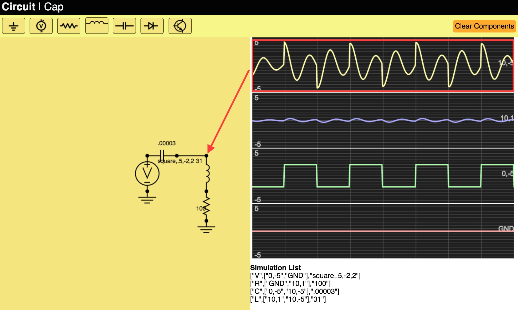
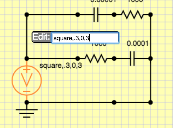
Using this we can now make a bridge rectifier circuit plus filter to turn AC into DC currents with minimal ripple.
bridgeRectFix

Graphing

The transient() function populates arrays for each value it is requested to collect. These are then send to the graph() routine which is basically a html5 canvas draw routine that puts those on the graphs on the right. See the code for more details, nothing super exciting there. I would like to make the graphing selective and have the ability to graph some quantities on the same graph window, but this suffices for now. I would also like to extend the simulator to produce currents for every element as well. That will likely require some rework to how the matrices are created which will make the union find from the last post less important.

Try it yourself

You can now try the program online at http://www.andyselle.com/circuit/.
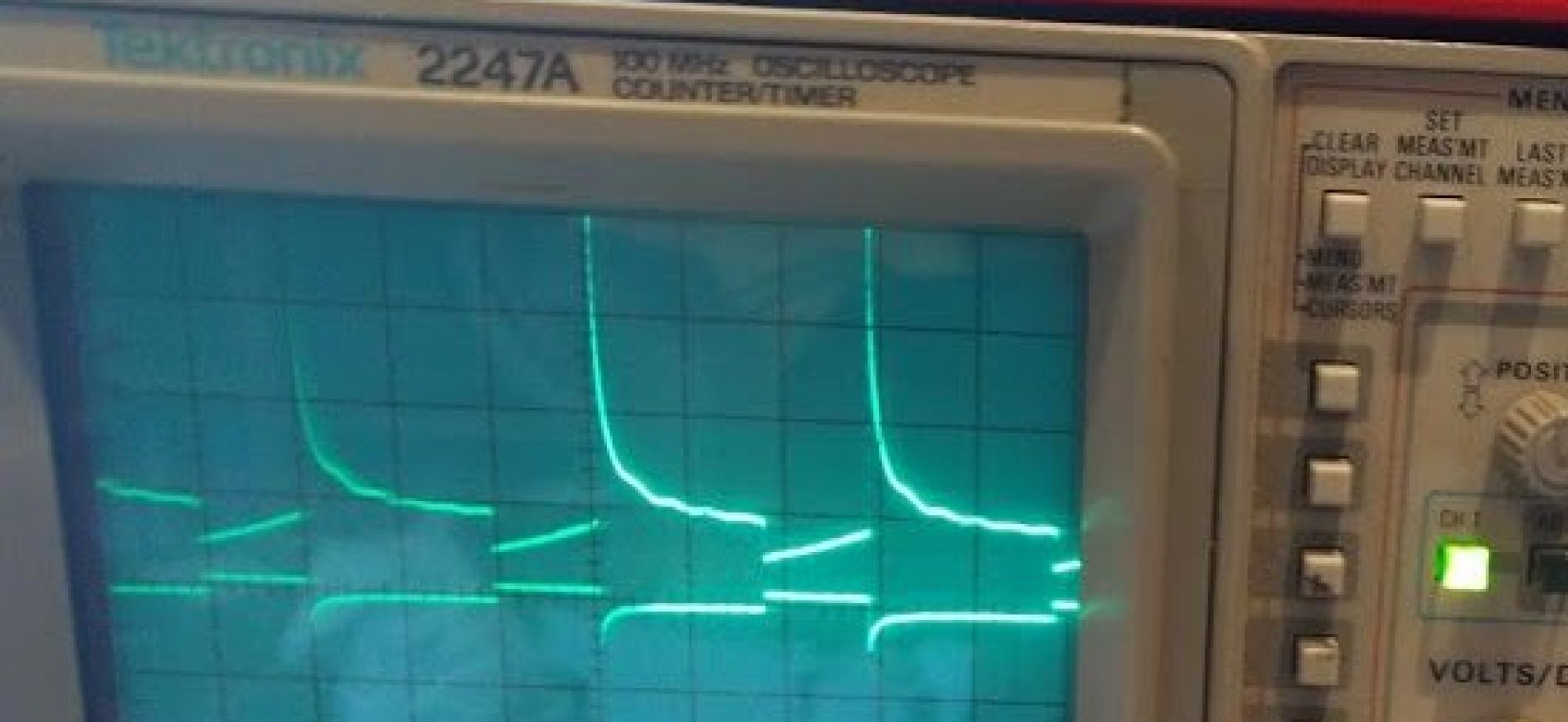
There is still a lot more to do to make this an awesome circuit simulator, but it’s basically working. Yay! Here’s another example I did with some weird non-linear inductor behavior
inductors


Circuit Simulation in Javascript Part III: Making the UI useful

Finally, I am picking up my long delayed circuit simulator. It’s been almost a year, so it is long overdue. There is no better time to do pointless educational programming projects than while vacationing. If you want to have a quick view of where we have gotten, see the youtube video at the bottom!

Anyways, in the part I we laid out the math for basic linear passives. In part II we made some of the UI for schematic capture. In this part we will advance the UI considerably. Below is a description of more problems we had to solve.

Adding components and adding wires

We now allow adding wires by clicking and dragging and we have a palette of components that can be added on demand. This was fairly uneventful. We also added “Backspace” and “r” as key options to delete and rotate the highlighted component.

palette

Managing connections

Allowing users to connect components is probably the trickiest part of the UI. The basic idea I came up with is to always assume we are on a grid. Every pin will always lay on exactly aligned to the grid. If two components pins are on top of each other then they are considered connected. Let’s get into the implementation.

To do this, we need a data structure that can map from a location to which component(s) (or at least how many) are incident at the location. A major design constraint is that we want it to be sparse, that is we don’t want a dense array of the grid nodes, so we actually implement this as a hash table. For simplicity we just consider the key of the hash table to be the string xCoord+”,”+yCoord (so it is human readable). Probably it would be more efficient to do some bit fiddly stuff like ((x&0xffff)<<16)+(y &0xffff), but we are just making something simple, so I’m going to punt on that aspect of performance.

Each UI operation will call functions on every editable component called buildNet(recordNet,unionNet). recordNet and unionNet are functions that the component can call to record any pin’s grid coordinates and unionNet let’s the component consider two grid coordinates to be connected (i.e. a wire uses these). For a resistor the buildNet() function looks like this:

ResistorSymbol.prototype.buildNet=function(recordNet,unionNet)
{
   var n1=recordNet(this.objectToWorld(0,0));
   var n2=recordNet(this.objectToWorld(10,0));
   return ["R",[n1,n2],this.value];
}

This registers the two pins of the resistor and returns a full description of the resistor for the net list (more on that later). The WireSymbol not only registers new nodes but also unions the two nodes into one conceptual node:

WireSymbol.prototype.buildNet=function(netRecord,unionNet){
   var n0 = netRecord(
             this.objectToWorld(this.points[0][0],this.points[0][1]));
   var n1 = netRecord(
             this.objectToWorld(this.points[1][0],this.points[1][1]));
   unionNet(n0,n1);
}

What does netRecord do? Basically it makes grid location based name and puts it into a hash table with the key being the name and the value being [<xcoord>,<ycoord>,<numberOfComponentPinsIncident>,<parentSet>]. xcoord and ycoord are obvious, <numbertOfComponentPinsIncident> allows us to draw an open circle when there is 1 unconnected pin, and a solid circle when everything is connected. Each component pin that touches this grid node increments that value. Lastly, parentSet is the name of the parent set in which we are contained. This will be explained below in the union set finding. The result of the buildNet() function is we have a data structure the UI can query when it is drawing to make open or closed circles at the pin locations.

connections

Creating the net list

Given a schematic, we would like to create a net list which is a description of what the components are and how they are connected. This is different than the schematic which has extraneous spatial information. For simulation we want a distilled description with only bare essentials needed for the simulator. In basic circuit analysis we use the lumped element model where any wire connections are assumed to be ideal. That means that any pins connected by wires become a single node. To accomplish this, we need to track connected components, so we will use a disjoint forest tree algorithm. For simplicity I am going to omit using the rank heuristic, but that would be easy to add to get the coveted inverse Ackermann function big-O performance. Remember the <parentSet> item in the node hash table discussed above. We start that equal to the key in the hash table. This means that the node is its own parent. Since everybody starts that way, everybody starts as a set of 1. Any unioning will change one of the parent entries to be the other. This implies trees and we can always find the effective name of the set by following parent links from a given node. To see this in action, consider this circuit where no unioning has been done:

step1

If we union one of the wire’s two pins we get:step2

If we union the other wire we get:step3

This is all good and find, but we actually need to handle GND specially.Anything that unions with GND gets parent being GND. GND basically has ultimate priority over everybody. To do this, we have a special GND entry.step4

After doing unioning of GND with its pin, we get this.
step5real

Now remember how components returned a simplified description. Those are always done in terms of immediate names. They aren’t the final unioned set representative. For example we would get [“R”,[“0,0″,”5,0”],1000] rather than the canonical effective names [“R”,[“0,0″,”GND”],1000]. So before display them, we need to lookup the final name by traversing the parent tree (this is the findSet() algorithm for disjoint forests).

Once we’re done with all this business, we can print out components we are interested in with lumped and unioned node names as shown below:

exampleUnioned

This representation is perfect, because we can use it to create a circuit simulation structure that actually can solve the circuit.

Editing component values

One last but important part is that we need some way to edit resistances, capacitances and set parameters for voltage sources. We could get arbitrarily complex, so for now, I am going to keep it simple. Every component just stores a string, and I can put whatever I want there. For the voltage source I am going to use <wavetype=sin|square|triangle>,<period in s>,<voltsMin>,<voltsMax>. Then, whenever somebody double clicks on a component, they will get an edit box to change the parameters. I might want to have more first class parameters types in the future, but this will get me by, and it took 5 minutes to implement! See here:

editor

Moving on

That’s probably enough for this time. I have made considerable progress on the simulator, and I will discuss how that was constructed in the next segment. To wet your appetite on how that works, take a look at this video of the simulator in action…

Clean Apple IIgs RGB and new workspace

Making a non-ghetto adaptor

In the previous post, I discussed my odyssey to have an Apple IIgs with a good RGB experience. My solution involved a vintage RGB CRT that my parents had squirreled away that I subsequently shipped across the country. I had developed an adapter PCB and had it fabbed using OSH Park. Unfortunately, I messed up, and the holes were too small for one of the parts. I bodged it all together using jumper wires to make sure the circuit concept worked but I was not happy with the result. Recently, I did a revision of the board to fix the hole spacing and physical issues, and sent it off to OSH Park. Here is the old vs new design

1st revisionpcb

new revisionOls
It just arrived back from OSH Park and I fitted everything together, and low and behold it fit. Following the datasheet physical dimensions in the CAD program amazingly works better than randomly choosing a hole size.  The following pictures show the soldered result, the adapter connected to the IIgs and my RGB monitor perched atop the IIgs.  It looks pretty good, but I don’t think that is exactly safe (especially in earthquake prone southern California. I think I’ll build/find a platform so that the computer can sit underneath the monitor but not support the weight.

Overall this has worked out really well, and I’m pretty happy with the result. If I have time and inclination, I may use this project as a chance to design a custom enclosure for the PCB for 3D printing.

An RGB display for an Apple IIgs

The impetus

I grew up with Apple IIs. My first home computer was an Apple IIc. While I had a love hate relationship with it, especially circa 1991-1992 when I wanted to have a “modern” PC or Mac at home instead of the very limited 6502 based system. Every now and then the nostalgia center of my brain sucks me toward Apple II emulators. Even so, the real thing is, well, cooler. My parents kept the Apple IIc and its excellent Apple composite color monitor, and one day, I will import that from Wisconsin to California (don’t tell my wife). Two years ago I acquired an Apple IIe and Apple IIgs from craigslist, and I was excited, because while I had used both machines back in the day, I had never owned them. I was especially excited about the Apple IIgs, because I wanted to try programming some of the Super hires graphics modes that I didn’t even know existed when I was programming basic (hell I didn’t even know that you could program double-hires).

Anyways, I brought those bad boys home and I got them running, transferred some disk images, and played around with them. Quickly two problems emerged: I didn’t really want to use floppies that much, and the scan converting box from my playstation 2 days was not going to cut it. 40 column and graphics was OK, but 80 column and Super Hires just sucked.

Ditching disks

The disk problem was the easier problem to solve. My dad brought me a back of 5 1/4″ disks and my favorite Apple II game Thunderchopper when he visited, so I was able to use ADT to bootstrap some disks. Not only were disks inconvenient. but I did not get a 3.5″ drive for my Apple IIgs, so I would be severely limited in what I could do with only a 5 1/4″.  I really wanted a Flash solution. The internet told me there was a great option the CFFA3000 (or video demo). I decided to put myself on the waitlist, and eventually I got it. It is an extremely well engineered piece of awesomeness, works perfectly, does everything I would want (except remote loading over ethernet). Here’s a picture of it in my IIgs.DSC_9531-11

I will remark that it is quite excellent in the IIgs where you can switch disks with Apple-option-escape, but it is a little clunky to use in an Apple IIe. This of course is not a workable solution in the Apple IIc where there are no expansion ports. Recently BMOW has been developing firmware to emulate floppy drives using the standard floppy connector. This is quite excellent too, but I am very happy with the CFFA 3000 right now.

Searching for a display

The search is not helped by the problem that RGB monitors in the mid-eighties were all slow-scan i.e. 15kHz rather than 31kHz. Most modern VGA monitors cannot sync to lower than 31kHz nowadays. You can use a scan doubler like NTSC TV signals can be scan-doubled in order to use them with a VGA display. There is also the question of CRT vs LCD. I thought I would never own another CRT again after ditching my ViewSonic CRT that didn’t withstand the UPS “fragile” shipping.

I needed something better. Basically, doing a ton of research on the internets led me to these possibilities

  • Find a 15khz monitor (AppleIIgs RGB, Amiga, Atari ST, Arcade CGA monitors could all work), but they are hard to find, expensive, and hard to ship.
  • Scan doublers like GBS-8220 can work, but are not considered very high quality.
  • Back in the day a VGA card for the Apple IIgs was created called the Secondsight, but it is rare and not fully compatible.
  • Early multisync VGA montiors do support 15 kHz, but they are very hard to find.
  • There are some LCDs that have SCART in the US, that work decently, but they are expensive and hard to find.

Needless to say, I was super discouraged at this point. I could throw money at the problem and buy a CRT, but it felt like a temporary solution. I was leaning toward the scan doubler approach, either building my own using an FPGA or using the GBS-8220. But, I didn’t have time so I put the project aside.

A plan forms

I was visiting my parents, and I realized they had a capable RGB monitor from the mid-eighties a Sony Trinitron KV-1311CR. This monitor was really quite nice in that had RGB, Composite and a cable tuner. In fact, I had used it in college as a television in my dorm room. The only problem was that it has this crazy RGB connector, a 34 pin ribbon DIP ribbon connector. (It also has that green RGB connector for digital (i.e. 8 colors) CGA displays).

DSC_9533-13DSC_9535-14

So, I just needed to find the pinout for this monitor and the Apple IIgs RGB port and make a converter. This turned out relatively easy  because it turns out “Don Lancaster’s Hardware Hacker” has an article on alternative RGB monitors for the Apple IIgs, and he has a diagram. He further says it’s an excellent monitor:

“The real winner seems to the be the great Sony KV-1311-CR monitor receiver. The praise lavished on this machine by the helpline callers was enough for me to actually go out and buy one for review and test.”

The big problem with using this monitor was getting it back to California intact. Moving CRTs requires lots of careful packaging. I used foam to pad the display, lots of bubble wrap before putting it into the box. Then I put that box in another box that was filled snugly with rolled up newspaper pages. Interestingly, the cheapest shipping option turned out to be checking it in my luggage (it cost only $35 (the price of an extra bag). Amazingly, it made it intact and working, though it looks like it was opened and searched (must be an uncommon item)/

The other big thing that I was concerned about was the pin numbering on the connector. I was concerned about how the pins were numbered on the ribbon connector. After scratching my head, the simplest way to figure it out was to find where the ground pins were (which I guess experienced people would say, duh, but hey I’m just a CS guy). So I just put my multimeter’s ground terminal onto the composite jack’s ground and found them. It turned out all the grounds were on one row (not the whole row, but almost). I can’t stress enough how frustrating this part was (doesn’t help to do this late at night). In fact, the numbering of the pins goes through one whole row and then to the other. This is different than an IDE which numbers swapping rows every pin number. I wanted to be absolutely sure, because I didn’t want to destroy a rare antique monitor by being careless.

The build

I have made cables many many times before. In fact, the first cable I made was an serial modem cable from Apple IIc DIN connector to IBM PC 9-pin connector to backup disks with ADT back in the 90’s. That cable was simply horrible (I didn’t even solder the wires because I didn’t have an iron or know how to solder). However, it did work. For this I wanted to do something a little more elegant. I figured I would create a PCB that had a male ribbon cable connector and the 15 pin male connector for the Apple IIgs side. Then, I can use a ribbon cable to connect to the monitor. If I get really clever, I could make a custom 3D printed cable housing for this. Doing a PCB for this does seem a little overkill, but it is not that crazy, considering OSHpark can produce boards dirt cheap, and I would need to find parts to make the hacked cable from anyways, why not do it right?

I’ve been using KiCad instead of eagle lately. Its routing is simply awesome compared to Eagle, but getting it setup is a real pain. Even so, I am very happy with it. Here is the basic schematic for the pinout. I really like making a schematic like this, because now I have documentation of how the cable works that I can share and refer to if anything goes wrong.

schematicI quadruple checked all the connections. A neat factoid here is that both the Apple RGB connector and the sony have a pin for audio, so I decided to include that. Pin 33 enabled analog RGB (rather than IBM CGA style TTL RGB). Pin 34 enables audio. The resistors in the divider here are not important, and in my implementation I used a 3k3 and 2k instead of 680 and 470. You just need to generate 5 volts. Ideally I would twist the signal specific GND’s, but I didn’t do that and it worked fine (see below).

The Build

Once I had designed the schematic I checked everything again, and I made footprints for the schematic symbols (I think how KiCad does this makes a lot of sense rather than the eagle method). This is where I made a mistake :(, but we’ll get to that in a second. Here is the completed route which was quite easy to do with the push and shove routing!

pcb


and here is the for-free 3D model that KiCad produces. One day I need to learn how to model things in Wings3D so I can see populated board previews.

pcbVizNow it was time to produce the board. This only requires one side, so I could easily etch it myself, but I have to get a drill press, and my VGA board was ruined twice by my inability to drill accurate holes. Doing dozens of pins that have to be exactly straight and aligned is really hard. Also, this board is really small, so it would only cost $5 to make with OSHpark. Furthermore, I was going on vacation to Utah for two weeks, so I was not in a hurry. So I sent it off before I went on vacation. When I got back, it had arrived and it looked like this

DSC_9538-16It looked awesome, and the Apple IIgs RGB D-SUB connector also had arrived and fit nicely

DSC_9514-1Unfortunately, the ribbon cable connector did not fit, because I had used the wrong hole size. The holes were too small. This was really frustrating, and it is exactly why I generally hate the idea of manufactured boards. It is too damn easy to waste your money! I didn’t really think I could drill the holes out to fix it, because there wasn’t really that much clearance, and again, I don’t have a drill press (or CNC). I settled with myself that I should just get another run done for only $5 dollars, but before I do that, I wanted to make sure things worked.

My solution was to wire wrap wires to the ribbon cable connector and solder those to the board. This sucked, but it wasn’t that bad, in that I decided I probably could get away with only 4 ground connections because there can’t be that much current….  DSC_9536-15Yes. This is ugly. I also plan on throwing it away once I get new boards made. I had also made one more error. The board was a little too wide and bumped against part of the Apple IIgs case, so I needed to cut a notch out of the board like this:

DSC_9515-2

Once I did that things fit perfectly

DSC_9516-3Before I plugged this into my monitor I used my voltmeter to make sure I was driving the last two pins with 5V only and I used my oscilloscope to make sure I was getting the correct signals on the correct pins. Everything looked great so I plugged it in and wrote a simple basic program to look at some colors

DSC_9518-5This is quite boring and doesn’t look as good in the photograph as it does in real life. Oregon trail happily works perfectly.

DSC_9525-8

I also ran some of the mac-like Apple IIgs software like AppleWorks GS

DSC_9528-9

It looks incredible and I am quite happy.

DSC_9532-12

Conclusion

So where does this all leave me. I made a working cable, but I need to edit my design and get new boards manufactured. Then I need to design an enclosure for the conversion PCB. I am quite happy with this way of making custom cables, and I might use it in the future for other similar tasks. I am sticking with KiCad for the long hall, though I might try Altium’s new tool just for fun. Using OSHpark was quite nice, and I will definitely use it again for small boards. For larger boards, I am inclined to try Elecrow, but we will see. I am also still inclined to make boards at home for prototyping, though if I am going to do anymore, I’m going to get a dremmel drill press jig, because my hands are not as steady as blondihack’s.

As far as my Apple IIgs. On the one hand, using this RGB monitor is still temporary, because it could easily fail, because all CRTs seem to be dropping dead. When that happens I can try my hand at learning CRT repair (e.g. recapping). Or, I can make a scan doubler at that point. Either way, I’m happy for now.

I need to make a custom stand to hold the monitor above the Apple IIgs, because the IIgs cannot safely support the larger KV-1311CR monitor. I would also like to find some solution for connecting the IIgs to the internet. I am thinking that PPP over a serial port is the most practical solution, but I haven’t looked into it carefully yet.


VGA Character Generator on an FPGA

In the last post we got our FPGA up and running and started generating VGA signals and some simple test patterns. Today, we want to work on character generation so we can actually display text. We’ll need to make  RAM to hold the character buffer (which will eventually be mutated by a CPU or some such thing). We’ll also need a ROM that stores the bitmap glyphs so that when we get an ASCII code from the the appropriate row and column, we can turn it into something that looks good. The basic block diagram for the approach is shown below:

vgaGenBlockDiagram

Before getting into the hardware programming of RAM and ROM (uncharted territory) I decided to do something easy. I fired up gimp and made a grid of 8×8 characters and started drawing characters. They are crappy, but they are mine.

charScreenshot

All good and fine, but I now need to turn this into a ROM. There are lots of ways of doing this, but since I am using the Altera FPGA tools I use the single port megafunction. This is nice and all, but it basically forces me to use some weird format for the binary data. I have a choice of two and I decide to use intel hex, because I found a python library that can generate then. Now I need to convert my font to .hex, so I write a python script that does this.   I followed a similar approach to make a RAM.

Now back to the hardware design. I’ll freely admit that I struggle trying to minimize the use of registers and try to use as much stuff that will synthesize into combinatorial logic rather than sequential. In fact, the character generator itself was a lot trickier than I expected. I ran into several problems.

First, I needed to change my VGA generation logic so that x was not completely invalid before getting into the active display region (non-blanking time). Specifically I needed to be able to compute the notion of “nextColumn” even before I was in a valid x coordinate. The easiest way I could think to do this was to initialize x to be 1024-8 (8 ints before it overflows). That way when I add to compute the “next x” I will get 0 when I am about to enter the active region. This sounds weird and stupid, and maybe it is, but it was essential and worked fine.  The “next” column of the character buffer (the one we need to load).

Second, I needed to be very careful about the timing. The idea is that each column of text takes 8 clocks to draw. I  need a register that holds one line of the character glyph steady for those 8 clocks (using a mux to choose which bit of the register to use). I basically can use the 8 clocks however I see fit. There are unfortunately some extra registers holding the address in the Altera FPGA mega structures (more on that later). That would be fine if they were controllable (i.e. if they had an enable bit). Instead, I have to make my own address registers which delays things one clock. Annoying. You can sort of see the dance of how things work in my annotated timing diagram below. I generated this by simulating using icarus verilog. That required me to make a fake RAM and ROM to replace the Altera mega functions, but that was a good exercise.

charGenWaveForm

Before I carefully sat down to think about the timing, I was getting all kinds of artifacts like the one shown below:

wpid-wp-1416908836301.jpeg

I found a major cause of these kinds of problems  was that in my generation of the RAM and ROM’s with the Quartus wizards, I had kept many default settings. One default setting is to have an extra register on the output of the RAM/ROM. This delayed the timing one more clock for no good reason. See the annoying setting below:

romNoWorks vs. romWorks

Unchecking that made things work better!

wpid-wp-1416908080633.jpg

At the end of all this I decided to make a simple white instead of cheesy rainbow colors. I also made a slightly more interesting message:

wpid-wp-1417677860356.jpg

I don’t know where I am going to go from here. An obvious thing to do would be to interface with a PS/2 keyboard or a serial port. If I did both I could make a simple dumb terminal. That could be kind of cool. Another cool thing to try would be to try to make a larger framebuffer (probably using external static ram) so I can do more interesting graphics. I might even add more rungs to my resistor DAC so I can get arbitrary colors. I could then implement a simple RAMDAC in the FPGA.


Basic VGA on an FPGA

I’ve been wanting to get into FPGAs for awhile. The fact that they are in a sense a very powerful carte blanche  for hardware projects is very tantalizing. A major motivation was the desire to understand video signal generation and to be able to do my own VGA projects. I was even thinking doing a scanline doubler for my Apple IIgs (with no RGB monitor) would be a great project.

To get started with FPGAs, I spent a bit of time looking into FPGA options. I really didn’t want to spend too much money but be able to do some reasonably sized. I settled on an older Altera EP2C5T144 clone. I downloaded it, learned a little Verilog and played with PCM blinking LEDs. I will spare you the details of getting the JTAG programmer to work with Ubuntu Linux (jtag needs to run as root). The Altera tools are a little complicated and clunky and compiling is quite slow on my 8 year old Linux box, but it works.

To take it to the next level, I knew I’d have to build some hardware to interface with a VGA port. I thought about it a bunch, designed a perfect R-2R resistor ladder that would take 3.3v in and have .7v nominal voltage when under a 75 ohm VGA spec load.  It seems like you should use opamp buffers or something, but I haven’t really searched hard for what the right chip for that would be. I also looked into DVI driver chips because the EP2CT5144 does not have the high speed differential outputs that I would need to reliably generate DVI. I actually picked up a few and I think when I do a real project, I’ll make a board that supports DVI and VGA for maximum awesome.  I thought about etching my own R-2R board that interfaces with my fpga, and I think that would be a good approach in the future.

Of course like most well-laid out hardware project plans I didn’t have time to do anything on this for a long time. I’ve been trying to cut down my internet “research” (watching other people do their own projects), but youtube is addictive.  Interestingly the reason I started this project was that my son has an obsession with helicopters that I thought would be well served by getting my dead battery containing Syma helicopter working. So, I figured that while I had my soldering iron out to fix the helicopter I should at least build the hardware for the VGA.

Since I had limited time, I decided to solder the minimum possible VGA board. The main question is what resistor to use for the RGB signals. I want a load 75 ohm to achieve about .7 volts so I have
 i_1 = i_2  \Rightarrow .7/75 = (3.3-0.7)/x \Rightarrow x=278\Omega \approx 270\Omega.
Given that we have this schematic:
fpga

That should give us about 8 colors. I’ll solder the leads and feed into a breadboard to put our resistors on. Then, we’ll connect to the EP2CT5144 dev board’s male jacks using a male to female ribbon connector.  (aside: The connectors and wires to use is always a part of electronics that I seem to do badly. In fact, I’d really like to know where I can find ribbon cable connector supplies, or if there is a good tutorial on what kind of connector stuff to use when). The finish product turned out crappy but workable as shown here:

DSC_3622-1

Of course I couldn’t really keep myself to working only the hardware at that point. I had been reading fpga4fun’s intro to VGA, and I had gotten that working to the point where it simulated ok. After hooking this up and reassigning the pins I thought it would just work. Of course it didn’t really work, and after a bunch of debugging, I found that I had swapped the hsync and vsync lines. So I fixed that, and it worked. Then I got to trying to draw a test pattern. I wasn’t really happy white the white level or the accuracy of the pixel placement (my LCD’s auto centering was totally flaking out), so I thought I’d have to play a little less fast and loose with the blanking portion.

I then wanted to be more precise about pixel locations and properly doing the front and back porch. I read the wikipedia page on VGA and I found that it would be smarter to do everything in terms of the pixel clock over the standard number of pixels. Then I played with it a bunch, and I really wasn’t super happy with the implementation. I wanted to try to do a better job of staying in spec, whereas fpga4fun plays really fast and loose, I only wanted to play kinda fast and loose. I modified the verilog implementation to do everything in terms of virtual pixel clock pixels.

Param Horizontal Vertical
Pixel clock 25.175MHz
Pixels 800 525
Sync range (in pixels) [16,112) [10,12)
Image range (in pixels) [160,800) [45,525)
Sync Frequency 25e6/800 = 31.25 kHz 25e6/800/525 = 59.52 Hz

Ideally this should be implementable with two counters and a state machine.  You could up the counters until they get to threshold for a given state and then transition. For now, I just went simpler and use 4 counters, two for the raw pixels and two for the visible pixels.  I am using all kinds of inefficient logic that probably creates adders to do comparisons, so I should try to optimize the number of gates down at some point. FPGAs really make it to waste lots of hardware, but that really is no different than writing in an inefficient scripting language on the software end. On the software side, I know better, I’m a newbie at hardware, so I’m sure I’m doing a lot wrong.

One big deal is this is the first project I’ve been working on using an oscilloscope. Debugging this with the oscilloscope was so much easier (and more fun), and I’m glad I waited to attempt this project until I got one.

pixelDataAndHsync signalGenerationHsyncVsync

Once the signals looked perfect and awesome, I decided to make sure I actually can see the full width of the screen, so I drew a box on the outer edge and I drew some colored boxes. I was having trouble with getting a proper full screen view on my LCD before my rewrite. Now it worked perfectly. Another improvement  that occurred from this rewrite was that the brightness of the whites improved (I had a very dim grey before).

While I was this far and it was only 1am, I decided to make another module that handles bouncing a ball. This was pretty easy, but I needed to make sure to denote my registers for pixel location as signed, so the twos complement addition for the velocity to position update. The final result showing the results is here:

DSC_3612-2

You probably want to checkout the youtube of this in action